Last updated: February 16, 2024
6 mins read
The Resonant Optical Cavity
The practical use of resonant optical cavities dates back to the Fabry-Perot Interferometer, devised by Charles Fabry and Alfred Perot, which is a fairly simple, but nevertheless ingenious, arrangement of two semi-transparent mirrors. See below for a great demonstration video from MIT, complete with a proper analog demo:
Today we have extremely large interferometers like LIGO, the gravitational wave detector, and microscale interferometers that can be fabricated in the thousands on a chip the size of the head of a pin.
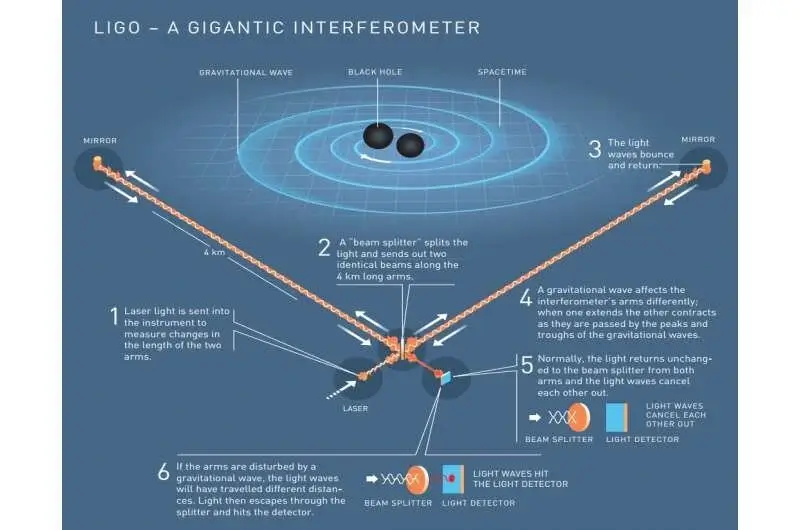
LIGO gravitational wave interferometer.
Due to constructive and destructive interference, certain wavelengths of light pass through a resonant cavity while others do not. The wavelengths that pass through the cavity are called resonance wavelengths, and when the optical path length in the cavity changes, these resonance wavelengths will also change.
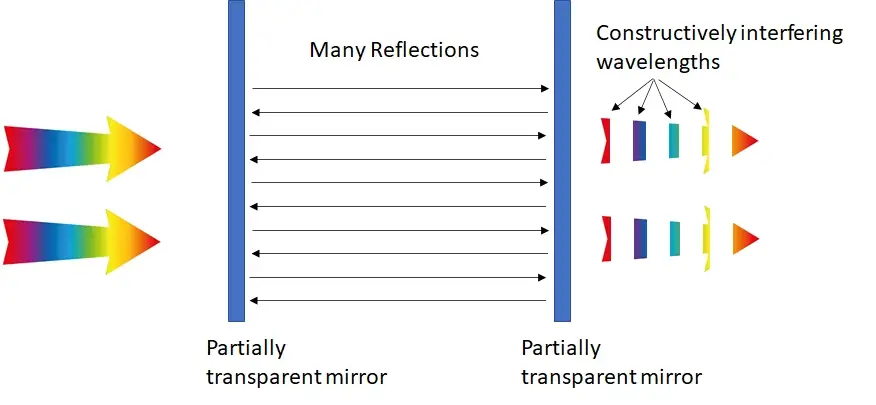
Note that the optical path length can be altered either by physically stretching or shrinking the path the light takes (which is what happens when gravity waves pass through the LIGO detector arms), or by changing the refractive index of the matter through which the light passes. Because the wavelength of light is on the order of 1 micron, or 1 millionth of a meter, even a tiny change in the optical path length changes the amount of transmitted light at a given wavelength.
Micro Ring Resonators
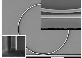
Silicon micro ring resonator (20 micron radius).[1]
The high sensitivity of optical cavities to the wavelength of incident light is widely used to create optical filters for fiber optic communications. When optical components began to follow the trend of chip-scale miniaturization, silicon micro ring resonators (MRRs) based on silicon nanowire waveguides became workhorse components of optical chips. See here for a basic explanation of total internal reflection and waveguides:
As seen in the electron microscope image above, a ring resonator is a looped silicon waveguide coupled to a straight waveguide. As light couples into the looped waveguide and back out again, it can accumulate exactly the right amount of phase to generate destructive interference in the straight waveguide’s output (see GIF below).
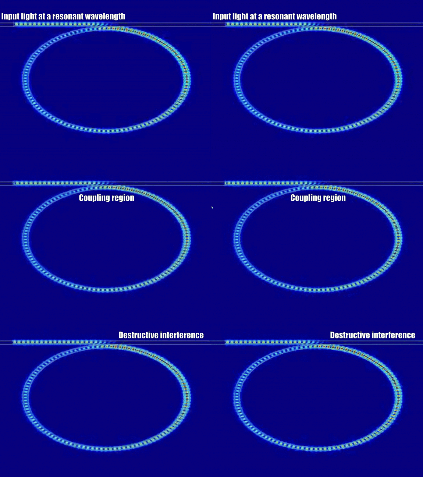
Electrical field in micro ring resonator at the resonance wavelength[2]
This results in an effect where some frequencies of light traveling in the straight waveguide are filtered out as they pass the ring. More on this in the next section. An excellent review of micro ring resonator theory can be found here: W. Bogaerts et. al
The working principle of MRR biosensors
The optical spectrum of a typical micro ring resonator is shown below (with periodic dips at the resonant wavelengths of light):
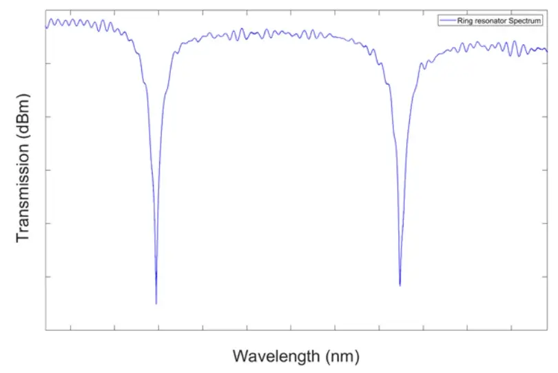
The distance between these periodic dips in a MRR’s spectrum depends on the ring’s overall optical path length (the longer the ring, the more wavelengths within a certain span fit into the ring an integer number of times, meaning there are more resonances), and changes gradually as the length of the ring is varied. However, the absolute position of the dips is highly sensitive to tiny changes in the refractive index of the ring. This is because light slows down when it passes through higher index material. For example, light is 30% slower in water than in air. If the light of a certain frequency circulating in the micro ring takes slightly more or less time to perform a full loop, it will no longer be at the correct phase to create destructive interference. The upshot is that a slightly higher refractive index causes the entire set of dips to shift to the right, and a slightly lower one causes them to shift to the left.
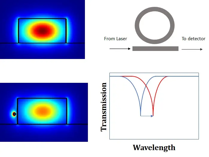
Left: Cross-section of a silicon waveguide with optical intensity Right: Schematic of resonance shift due to particle attachment to the waveguide surface
As light travels through the silicon nanowire, about 30% of it interacts with what is called “the cladding.” The cladding is a low index medium like glass, air, or water, that leads to total internal reflection at the interface with the silicon waveguide. In telecom applications, a glass cladding is typically used, but to build a biosensor, the glass cladding over the micro ring is intentionally omitted (in reality it is etched away after deposition).
This allows the ring to be exposed to liquid samples. And as analyte molecules bind to the surface of the waveguide, the spectrum of the ring shifts to the right:
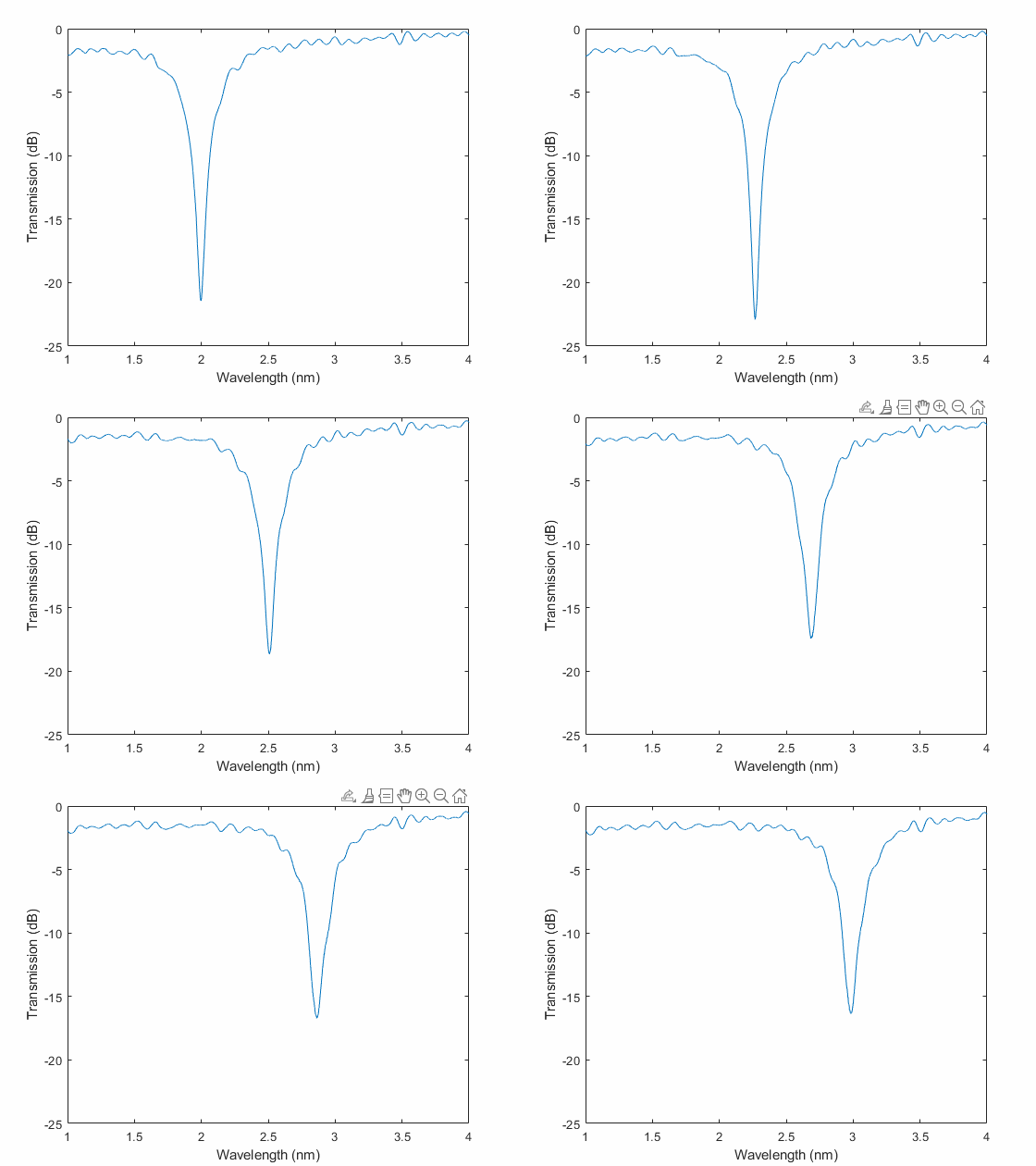
Optical spectrum of a micro ring resonator red shifting due to the SARS-CoV-2 nucleocapsid protein attaching to the waveguide surface.
The sensitivity of MRR sensors comes from the optics (and they can be sensitive down to detecting a single nanoparticle), but the specificity comes from the surface chemistry. Surface capture proteins (e.g. antibodies) are typically attached to the sensor in order to make it specifically capture a certain target. For example, attaching anti-spike antibodies to the MRR surface makes it sensitive to SARS-CoV-2 viruses. By printing different proteins, DNA probes, or other chemistries onto different rings, it’s possible to detect a large number of analytes in a tiny sample. Each ring can be as small as ~5 microns in radius (the minimum bend radius that doesn’t allow light to leak out of the sides of a silicon waveguide), meaning that thousands can fit into a square millimeter. See the GIF above for real-time data from the detection of COVID nucleocapsid protein with a micro ring.
Scalability Matters
There are many highly sensitive optical approaches (such as various ELISAs and molecular assays based on fluorescence and chemiluminescence) to detect proteins and nucleic acids. What makes silicon micro ring biosensors unique is their scalability and low cost. By using a sensor that is compatible with production in standard large-scale semiconductor fabs (silicon photonics products are made in the millions for the telecom and datacom industries), it’s possible to build a massive amount of tests in a very short time, at very low cost.
A rough breakdown:
Each 12-inch SOI wafer can produce 70,000 square-mm chips.
Individual MRR biosensors occupy at most .01 square-mm, meaning that a 1 mm * 1 mm chip can have dozens or even hundreds of individual sensors.
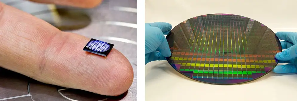
A single semiconductor fab can produce up to 100,000 wafers a month. Note that this is 100,000 full semiconductor process wafers. MRR sensor chips only require a small subset of the process steps used for typical chips, meaning that capacity for producing sensors is actually much higher.
This means that 7 Billion sensor chips can be produced at a single semiconductor fab each month at a cost that could be as low as 25 cents per chip.
SiPhox
We’re hard at work commercializing SiPhox Home, a versatile handheld at-home diagnostics platform. Initial cartridges will perform a low-cost and highly scalable COVID test, followed by a range of common diagnostic tests for biomarkers and infectious diseases.
Are you an A+ engineer or scientist with systems, electro-optics, photonics, synthetic biology, microfluidics or assay development experience? See here for open positions.
References


